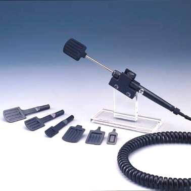
日本Fluoro Mechanic晶圆搬运真空棒

Vacuum Wand for Wafer Handling晶圆搬运真空棒Our unique valve*ensures reliable suction and release of a semiconductor wafer.我们独特的阀门*确保对半导体晶圆进行可靠的吸附与释放。The well polished inner wall of the valve part minimizes

Vacuum Wand for Wafer Handling 晶圆搬运真空棒

  • Our unique valve* ensures reliable suction and release of a semiconductor wafer.我们独特的阀门*确保对半导体晶圆进行可靠的吸附与释放。

  • The well polished inner wall of the valve part minimizes particle generation.阀门部件内壁抛光精良,可*大程度减少颗粒产生。

  • The optically polished wafer tip provides excellent adhesion to a wafer.光学抛光的晶圆**能与晶圆实现**的贴合。

  • The vacuum wand body can be easily detached from the tubing.真空棒本体可轻松与管路分离。

*US Patent 6176265B1, Japanese Patents 1698352/1885465*美国**第6176265B1号、日本**第1698352号/第1885465号

You can find the vacuum wand which meets your requirements on our interactive catalog.你可以在我们的交互式产品目录中找到满足你需求的真空吸棒。

Vacuum Wand C series for ESD protection用于静电防护的真空吸笔C系列
ESD Safe Vacuum Wand (Vacuum Pen, Vacuum Tweezers) for Semiconductor Wafer Processing: The wafer tip is made of Conductive PEEK. Vacuum pens for SMD/die handling are available.
  • The body covered with Conductive Nylon reduces electrostatic effects towards a wafer.包覆有导电尼龙的本体可降低对晶圆的静电影响。

  • The wafer tip is made of Conductive PEEK (Polyetheretherketon).晶圆**由导电聚醚醚酮(PEEK)制成。

  • The resistance value of 106 to 108 ohms provides optimum static protection.106至108欧姆的电阻值可提供*佳的静电防护效果。

  • For 5, 6, 8 and 12-inch wafer handling适用于5英寸、6英寸、8英寸和12英寸晶圆搬运


首页
产品
新闻
联系